News Release
Opto Diode Corporation
An ITW Company
1260 Calle Suerte
Camarillo, CA 93012
Contact: Russell Dahl, Business Unit Manager
Phone: 1+ 805.499.0335 x312
Fax: 1+ 805.499.8108
Email: russdahl@optodiode.com
Website: www.optodiode.com
Media Contact: Marlene Moore
Smith Miller Moore
Phone: 1+ 818.708.1704
Email: marlene@smithmillermoore.com
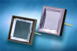
Opto Diode Introduces 13.5 nm Directly-Deposited Thin-Film Filter Photodetectors
CAMARILLO, Calif. - December 11, 2017 - Opto Diode Corporation, an ITW company, introduces the SXUV100TF135 and SXUV100TF135B photodiodes with integrated thin-film filters. The detectors each feature a 100 mm2 active area and a directly-deposited thin-film filter for detection between 12 nm and 18 nm.
Both detectors have typical responsivity of 0.09 A/W at 13.5 nm and are optimized
for different electrical performance. The photodiodes are ideal for use in applications such as laser power monitoring, semiconductor photolithography, and metrology systems that utilize extreme ultraviolet light.
Opto Diode Corporation (Camarillo, CA - www.optodiode.com), an ITW Company, delivers industry-leading sensors, photodiodes, IR detectors, photonic modules, assemblies, and LEDs. Available in standard and custom designs, Opto Diode products have earned a reputation for high performance, superior quality and reliability for over 30 years. Opto Diode offers advanced performance sensors from the extreme ultraviolet (UV) to the mid-infrared (mid-IR). Our products provide unparalleled high-energy particle, electron, X-ray, and UV detection along with superior sensitivity to discriminate trace gases or detect heat, sparks, or flames in the mid-IR spectrum. Other products include high performance LEDs with radiometric emissions from 365 to 940 nm and IR emitters covering 1 to 10 microns.
Opto Diode serves a variety of industries including aerospace, automotive, biotechnology, food processing, medical, military/defense, industrial, semiconductor equipment manufacturing, and test & measurement. Our manufacturing process is in a cleanroom environment, from start to finish. Opto Diode’s domestic U.S. facility is optimized for design and manufacturing with an on-site wafer fabrication, class 1,000 to class 10,000 clean rooms, extensive assembly capabilities and packaging expertise. From prototyping to high-volume production, we manufacture wafers-to-components then package and assemble photonic modules-to-optoelectronic sub-systems. For more information, visit www.optodiode.com.

