Resources: Photoconductive Infrared Detectors and Emitters - Technical Notes - Bias
To define Bias Required from Signal Processing Electronics
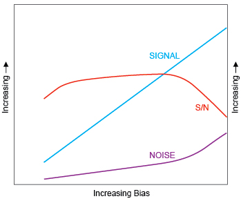
In general, signal is linearly related to bias voltage (up to approximately the detector maximum bias voltage). At low bias, PbS/PbSe detector noise shows relatively little dependence on voltage. After a given voltage value is reached, noise is linearly related to voltage. The typical variation of signal, noise and S/N of PbSe detectors with bias is shown in the figure below. Larger detector areas require higher bias voltage to reach this range.
Detector noise is a function of the inverse of the chopping frequency. Therefore, at decreasing chopping frequencies further decreased voltage bias may yield acceptable signal to noise ratios.
Note: bias values left undeclared in above graph as optimal bias depends on detector active area size.
Opto Diodes’ standard test rules are 50 VDC per mm between electrodes for PbS cooled and uncooled (A type detector), 35 VDC per mm between detector electrodes for PbSe uncooled (BX detector type), 25 VDC per mm between detector electrodes for PbSe cooled (BX detector type).
Example: a PbSe uncooled (BX type) 2x2mm detector has a 2 mm active area between electrodes, and would therefore be tested with 70 VDC bias.

