
Photodiodes for Microscopy and Nanopositioning Applications
Precision Optical Detection for Microscopy and Nanopositioning
Microscopy and nanopositioning systems require detectors that can measure extremely small optical signals with stability and accuracy. In microscopy, the detector may need to capture low-light signals from fluorescence, confocal, light-sheet, or super-resolution systems. In nanopositioning, the detector may need to resolve tiny beam-spot shifts for AFM cantilever deflection, autofocus, beam centering, and optical alignment.
In both cases, performance depends on more than peak responsivity. Engineers must also consider detector geometry, wavelength range, dark current, noise, package stability, thermal drift, and front-end electronics.
Why Detector Geometry Matters
The right detector starts with the measurement type.
For intensity-based measurements, such as fluorescence detection, brightfield monitoring, and confocal microscopy, a single-element photodiode is often the best fit. Blue-enhanced silicon photodiodes can support UV and blue fluorescence applications, while red-enhanced silicon photodiodes are suited for red and near-infrared emission bands.
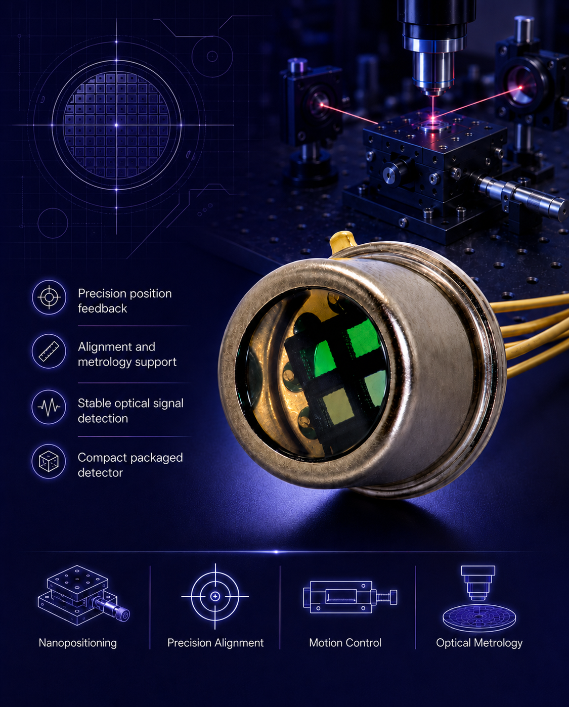
For position-based measurements, such as AFM deflection, autofocus, or beam centering, segmented photodiodes are often preferred. A bi-cell detector supports single-axis focus tracking, while a quad-cell detector provides two-axis beam-position feedback.
Because bi-cell and quad-cell detectors use matched elements on a common substrate, they can provide better stability than discrete photodiodes arranged separately.
Quad-Cell Detectors for AFM and Beam Centering
Quad-cell segmented photodiodes are commonly used when an optical system needs to track beam movement across two axes. In AFM beam-deflection systems, a laser reflects from the cantilever onto a segmented detector. As the cantilever moves, the beam position shifts across the quadrants, producing differential signals used for position feedback.
Common-substrate quad-cell detectors help reduce quadrant mismatch, centering error, and thermal drift. This makes them useful for AFM, SPM, optical alignment, beam centering, and precision metrology systems.
Bi-Cell Detectors for Autofocus and Single-Axis Tracking
Bi-cell photodiodes are used when the system only needs one-axis feedback. In autofocus applications, the detector compares the output from two matched elements to generate a focus-error signal.
This makes bi-cell detectors useful for single-axis nulling, focus tracking, and alignment systems where long-term stability is important.
APDs for Low-Light Confocal Detection
Confocal microscopy and FLIM applications often operate in photon-starved conditions. When the optical signal is too weak for a standard PIN photodiode, an avalanche photodiode, or APD, can provide internal gain to help raise the signal above the readout noise.
Silicon APDs support visible and near-infrared detection, while InGaAs APDs support NIR and SWIR applications from approximately 900 nm to 1700 nm.
Opto Diode Detector Families for Microscopy
Opto Diode supports several detector families for microscopy and nanopositioning applications, including:
Blue-enhanced silicon photodiodes: UV and blue fluorescence, brightfield detection, and short-wavelength emission bands.
Red-enhanced silicon photodiodes: Red and NIR fluorescence, laser monitoring, and visible-to-near-infrared detection.
Silicon APDs: Low-light confocal microscopy, FLIM, and photon-starved visible/NIR detection.
InGaAs APDs: NIR and SWIR microscopy or spectroscopy from 900 nm to 1700 nm.
Bi-cell segmented detectors: Autofocus, one-axis nulling, and single-axis beam tracking.
Quad-cell segmented detectors: AFM cantilever deflection, beam centering, optical alignment, and two-axis position feedback.
Custom Detector Options
Some microscopy and nanopositioning instruments require custom detector designs. Opto Diode can support custom active-area geometries, gap widths, quadrant layouts, multi-element detector configurations, array detectors, integrated TIA amplifier hybrids, and hermetic, windowless, or filter-integrated packages.
These options are useful when an instrument has specific beam-profile, wavelength, resolution, package, or long-term stability requirements.
Talk to Opto Diode About Your Application
Selecting the right photodiode starts with the measurement. For microscopy, define the wavelength band, expected signal level, active area, noise floor, and bandwidth. For nanopositioning, define the beam profile, spot size, detector geometry, gap width, and stability requirements.
Opto Diode’s Applications Engineering team can help recommend a standard detector family or review a custom detector path for your system.
What's Latest


Get a Quotation Now
For any queries, please complete the form and we
will contact you within 48 hours